Alliages de Substitution
pour les Productions Electroniques:
Alliages et température de fusion : (Lingots, barres,
baguettes, grenailles, Préformes fils)
Crèmes à braser (pâtes & encres)
LEAD FREE SOLDERS IN ELECTRONICS
• Greater Thermal Stress of Components
• Use of Temperature Sensitive Components and
LEAD FREE
ALTERNATIVE SOLDER ALLOYS
DISSOLUTION
KINETICS OF COPPER
THE EFFECT
OF ISOTHERMAL AGING
Integrity of Solder Joints
from Lead-free Solder Paste
• Greater Thermal Stress of Components
LEAD FREE
ALTERNATIVE SOLDER ALLOYS
96.2Sn/2.5Ag/0.8Cu/0.5Sb (known as Castin) 217-220 °C
90Sn/2.0Ag/7.5Bi/0.5Cu (138) 198-212°C
DISSOLUTION
KINETICS OF COPPER
THE EFFECT
OF ISOTHERMAL AGING
2. Alternative
materials and solder
3. Oxidation
tendency of different
5. Low-melting
binary and ternary
7. Alternative
surface metallizations
Alliages
de Substitution pour les Productions Electroniques:
Alliages et température de fusion : (Lingots, barres, baguettes, grenailles, Préformes fils)
|
Ref. |
composition |
Liquidu |
Solidus |
densté |
|
§ S 100 |
Sn100 |
233 |
E |
7,80 |
|
§ |
Sn90 |
Ag10 |
300 |
227 |
7,32 |
|
§ SA 2.5 |
Sn97,5 |
Ag2,5 |
226 |
221 |
7,34 |
|
§ SA 3 |
Sn97 |
Ag3 |
232 |
E |
7,28 |
|
§ SA 3.5 |
Sn96,5 |
Ag3,5 |
221 |
E |
7,36 |
|
§
SA 5 |
Sn95 |
Ag5 |
240 |
232 |
7,25 |
|
§
SA 5 |
Sn95 |
Ag5 |
222 |
183 |
7,42 |
|
§ SB 40 |
Sn60 |
Bi40 |
170 |
138 |
8,12 |
|
§ SB 5 |
Sn95 |
Sb5 |
248 |
179 |
8,43 |
|
§ SC 0,7 |
Sn99,3 |
Cu0,7 |
227 |
E |
|
|
§ SC 3 |
Sn97 |
Cu3 |
320 |
227 |
|
|
§ SI 42 |
Sn58 |
In42 |
145 |
118 |
7,30 |
|
§ SI 48 |
Sn52 |
In48 |
131 |
118 |
7,30 |
|
§ SS 2 |
Sn98 |
Sb2 |
240 |
221 |
7,39 |
|
§ SS 3 |
Sn97 |
Sb3 |
240 |
235 |
7,28 |
|
§ SZ 9 |
Sn91 |
Zn9 |
199 |
E |
7,27 |
2°) Alliages tertiaires:
|
§
SAB |
Sn |
Ag |
Bi |
|
|
|
|
§
SAC 305 |
Sn96,5 |
Ag3,0 |
Cu0,5 |
217 |
218 |
7,39 |
|
|
Sn95,75 |
Ag3.5 |
Cu0,75 |
217 |
|
7.38 |
|
§ SAC 385 |
Sn95,7 |
Ag 3,8 |
Cu0,5 |
|
|
|
|
§ SAC 387 |
Sn95.5 |
Ag3.8 |
Cu0.7 |
217 |
E |
|
|
§ SAC 408 |
Sn95,2 |
Ag4 |
Cu0,8 |
|
|
|
|
§ SAS 25.10 |
Sn65 |
Ag25 |
Sb10 |
238 |
232 |
7,26 |
2°) Alliages quaternaires:
|
§ SABC |
Sn |
Ag |
Bi |
Cu |
|
|
|
|
§ SAC 0307 Co |
Sn98,07 |
Ag0,3 |
Cu0,7 |
Co 0,03 |
217 |
227 |
7,32 |
Ces
changements peuvent imposer des modifications importantes au niveau
des process, des équipements, et des composants.
En contrepartie, les
alliages "Sans Plomb" présentent une meilleure résistance
au fluage et des caractéristiques de tenue mécanique plus élevées
que l'alliage Sn63Pb37.
|
Désignation de l'alliage |
Zone de fusion |
Poids. |
|
|||
|
Alliages
sans plomb RoHS |
Solide |
Liquide |
spéc |
Domaines
d'utilisation |
|
|
|
|
Sn 97 Ag2 Cu Sb |
216 °C |
221 °C |
7.3 |
Soudure fine sur C.I. - Soudage de composants pour constructions radio, télévision, retouches, trous métallisés. Soudure pour professionnel, câblage conventionnel. - Appareil de mesure. - Circuits imprimés cuivre nu. - Améliore la résistance mécanique. Soudage sur circuits dorés, céramiques argentées et toutes bases argentées. - Soudure utilisée pour des ensembles travaillant à des températures élevées (lampes, moteurs,…) Soudure sur céramique argentée, circuits imprimés, basse température, points juxtaposés. Soudure spéciale pour grande résistance mécanique. - Soudures sans plomb pour contact alimentaire. |
|
|
|
Sn 96 Ag |
221 °C |
eutectique |
7.3 |
||
|
|
Sn 100 |
232 °C |
Fusion |
7.3 |
||
|
|
Sn 97 Cu Sn 99 Cu |
227 °C 227 °C |
320 °C eutectique |
7.3 7.3 |
||
Crèmes à braser (pâtes & encres)
Tableau
des Crèmes
Le monde
du "sans plomb" regorge d’acronymes, d’abréviations et de
termes qui ne vous sont peut-être pas familiers. Grâce à cette page,
nous ferons de notre mieux pour lever le voile sur vos doutes et vos
interrogations compte-tenu de l’évolution de la législation RoHS.
|
Acronyme |
Définition |
Signification |
|
ASO |
Ag / Sn / O2 |
Oxyde d'Etain/d'Argent |
|
SAC |
Sn / Ag / Cu |
Alliage Etain Argent Cuivre |
|
SAB |
Sn / Ag / Bi |
Alliage Etain Argent Bismuth |
|
SABC |
Sn / Ag / Bi / Cu |
Alliage Etain Argent Bismuth Cuivre |
|
SAC408 |
Sn / Ag 4% / 0,8% Cu |
Alliage mixte |
|
SAC385 |
Sn / Ag 3,8% / 0,5% Cu |
Alliage mixte |
|
SAC305 |
Sn / Ag 3,0% / 0,5% Cu |
Alliage mixte |
|
NiAu |
Nickel / Or |
|
|
Pb |
Plomb |
Symbole chimique |
|
Cd |
Cadmium |
Symbole chimique |
|
Hg |
Mercure |
Symbole chimique |
|
Sn |
Etain |
Symbole chimique |
|
Ag |
Argent |
Symbole chimique |
|
Bi |
Bismuth |
Symbole chimique |
|
Cr (VI) |
Chrome hexavalent
|
|
|
PBB |
Biphényles polybromés
|
Ignifugeants |
|
PBDE |
Diphényléthers polybromés
|
Ignifugeants |
|
BGA |
Boîtier à matrice de billes |
|
|
CSP |
Boîtier-puce |
|
|
CRT |
Tube cathodique |
|
|
DTI |
Ministère britannique du Commerce et de l’Industrie
|
Ministère clé chargé de promouvoir la mise en
conformité avec la Directive RoHS
|
|
DEFRA |
Ministère britannique de l’Environnement, de
l’Alimentation et des Affaires rurales |
Ministère de l’environnement |
|
CE |
Commission européenne |
|
|
ED-XRF |
Analyse par fluorescence X à dispersion d'énergie
|
|
|
ELV |
Véhicules hors d'usage |
Directive de l'Union européenne |
|
ESH |
Environnement, Sécurité et Hygiène |
|
|
HASL |
Nivellement de la soudure à l'air chaud |
|
|
IT |
Technologie de l'information |
|
|
LFS |
Soudure sans plomb |
|
|
MCV |
Valeur de concentration maximale |
|
|
MLCC |
Condensateurs céramiques multicouches |
|
|
m.pt. |
Point de fusion |
|
|
MSL |
Niveau de sensibilité à l'humidité |
|
|
OEM |
Equipementier |
|
|
PCB |
Carte imprimée |
|
|
PVC |
Chlorure de polyvinyle |
|
|
QA |
Assurance Qualité |
|
|
RoHS |
Restriction de l'utilisation de certaines substances
dangereuses |
Directive de l'Union européenne |
|
SME |
Petites et moyennes entreprises |
|
|
TAC |
Comité d'adaptation technique |
Comité technique de l'Union européenne |
|
TCF |
Dossier de conformité technique |
|
|
VOC |
Composé organique volatil |
|
|
WD-XRF |
Analyse par fluorescence X à dispersion de longueur
d'onde |
|
|
DEEE |
Déchets d'équipement électrique et électronique
|
Directive de l'Union européenne |
LEAD FREE SOLDERS IN ELECTRONICS
Angela Grusd
Heraeus Inc.
West
Lead-bearing solders are used extensively in the electronics
industry. In recent years, efforts to develop alternatives to lead-based
solders have increased significantly. As researchers began to focus
on Pb-free solders they recognised their
potential in high temperature applications such as automotive where
Sn/Pb solders do not meet the demanding
requirements. In particular, the Sn-Ag-X lead free solders offer superior creep resistance
at room temperature and 100°C as
compared to Sn-40Pb. Results of this work will be presented as well
as factors to consider when developing
and implementing lead free alloys such as manufacturability,
availability, and cost. One of the most promising replacement alloys
is Sn/4Ag/0.5Cu. This alloy will be discussed in detail.
Lead free solders are currently in production in some
facilities and some of the “green” companies have proposed timelines
for their implementation in the next year. The development of lead
free lternatives was initially driven by impending
Automobile Industries Association. This called for a
50% voluntary reduction of lead in vehicles (excluding batteries)
by 2001 and to one-third by 2003. Several major Japanese Consumer
Electronic Manufacturers have publicly announced accelerated plans
to eliminate lead solder completely by 2001. Lead free alternatives
are being considered for several reasons:
• Health Concerns
It is widely known that lead is related to certain health
risks. If lead particles are inhaled or ingested, they accumulate
in the human body causing damage to the blood and central nervous
systems. Lead poisoning can be detected by blood analysis and the
limits are defined by national governments.
The standard upper value of untainted human beings should
not exceed 130 µg/l. The upper blood lead limit of people who are
exposed to lead at work is, according to the
As a result, some industries have already eliminated
lead and have found suitable alternatives, for example plumbing solders,
tinned cans, lead-free gasoline for vehicles, and leadfree
cut crystal glass. The majority of lead consumption is automobile
batteries and ammunition. The lead consumption of the electronics
industry is relatively small and, according to different sources,
lies between 0.5 - 7%.
When choosing alternative metals, consideration must
also be given to their health risks as well. Recent studies in the
the toxicology of lead and some alternative metals:[1]
• Cd is extremely toxic and
should not be used (high risk). Many companies such as Ford Motor
Company have banned Cd-containing materials.
• Pb was also identified as
highly toxic (high risk - it is considered harmful to the reproductive
system).
• Sb is very toxic and should
not be considered a major alloying element (medium risk - in
• Ag and Cu are used in lead-free alloys in small concentrations
- in
• Sn and Zn are essential elements
in the human diet, yet may be toxic if exposures are sufficiently
high (low risk).
• Bi is a relatively benign metal with a history of medicinal
uses (low risk).
• Greater Thermal Stress of Components
In the automotive industry, more and more circuits are being
placed in the engine compartment in order to reduce the
quantity of cables and, therefore, reduce cost. These under
the hood conditions often see temperatures in excess of
150°C. A leading automobile manufacturer has even
measured temperatures as high as 170°C on a hybrid circuit.
The high thermal stresses imposed on the solder joints at
these temperatures has led automotive manufacturers to
research Pb-free alternatives with high thermal
fatigue
resistance, because they observed that Sn-37Pb has poor
thermal fatigue properties even at 125°C. Higher
temperatures dramatically reduce the strength of the
solder joint during thermal cycling, due to greater plastic
deformation of the solder as well as diffusion,
recrystallization and grain growth
inside the solder.
For conventional alloys such as Sn62/Pb36/Ag2 (melting
point 179°C) and Sn63/Pb37 (melting point 183°C),
there is a major concern for the mechanical and
microstructural stability and,
therefore, the reliability of
the solder joint at an operating temperature of 150°C,
because it is approaching the melting point of the alloy.
• Use of Temperature Sensitive Components
and
Some industries have driven down costs by replacing
higher cost plastic components with less expensive
plastic ones. These components, however, cannot
withstand the standard reflow temperatures of
210-
230°C. Therefore low melting temperature solder alloys
are used in this case. This is especially apparent with
consumer electronics, as the operation temperatures are
from 0°C to +60°C. This lower temperature range
corresponds to much less thermal stress on the solder
joints as compared to those temperatures found in underthe-
hood applications which typically reach 150°C or
greater. An example of a solder for these lower
temperature applications is Sn/Bi eutectic.
LEAD FREE ALTERNATIVE SOLDER ALLOYS
1. Sn/Ag (96.5Sn/3.5Ag:221°C)
This alloy exhibits adequate wetting behavior
and
strength and is used in electronics as well as plumbing.
Several sources have also reported good thermal fatigue
properties as compared to Sn/Pb. Thermal fatigue
damage in solders is accelerated at elevated temperatures.
In the Sn/Pb system, the relatively high solid
solubilities
of Pb in Sn and vice
versa, especially at elevated
temperatures, lead to microstructural instability
due to
coarsening mechanisms. These regions of
inhomogeneous microstructural coarsening are
known to
be crack initiation sites. It is well-documented that these
types of microstructures in Sn/Pb alloys fail
by the
formation of a coarsened band in which a fatigue crack
grows. By comparison, the Sn/Ag system, has limited
solid solubility of Ag in Sn, making it more
resistant to
coarsening. As a result, Sn/3.5Ag eutectic forms a more
stable, uniform microstructure that is more reliable.
Although the Sn/3.5Ag alloy itself exhibits good
microstructural stability, when
soldered to copper base
metal, the combination of a higher Sn content
(96.5Sn
compared to 63Sn) and higher reflow temperature
environments accelerate the diffusion rates for copper base
metal in Sn. As its corresponding composition
is reached, the
brittle Cu6Sn5 intermetallic compound is nucleated
and begins
to grow. To slow the diffusion rate and thereby decrease the
growth kinetics, alternative surface finishes such as
immersion gold (Au over Ni over Cu) may be used. The 2 µm
Ni in the immersion gold coating serves as an effective
diffusion barrier, limiting the Cu from diffusing into the
solder and forming the brittle Cu6Sn5 intermetallic compound.
Other surface finishes such as immersion silver (Ag over Cu)
and immersion palladium (Pd over Cu) do not contain a Ni
barrier layer. Their effect on the growth kinetics of the
intermetallic compound layers
is under investigation.
1) 95.5Sn/4.0Ag/0.5Cu
217-219°C
2) 95.5Sn/3.8Ag/0.7Cu
217-219°C
3) 95.0Sn/4.0Ag/1.0Cu
217-219°C
4) 93.6Sn/4.7Ag/1.7Cu 216-218°C
Because the mechanical stability of the joint is degraded when
the melting point is approached, elevated temperature cycling
produces more damage for Sn/Pb solder (m.p. 183°C) as
compared to higher melting point solders. The melting
temperatures of Sn/Ag/Cu solders make them ideal
in high
operating temperatures up to 175°C. As for wetting,
Sn/Ag/Cu solders do not wet
Cu as well as Sn/Pb using
commercial fluxes. However, good fillet formation can be
easily achieved provided the fluxes are suitable for higher
temperature use. Soldering in nitrogen atmosphere also
improves wettability using no-clean fluxes. The
copper
dissolution test provides a relative measurement of the
solder’s tendency to dissolve Cu from the base metal and
form the Cu6Sn5 intermetallic compound. For
alloys 1-3, the
rate of copper dissolution is slower than the Sn/Ag
alloy yet
faster than the Sn/Pb eutectic. For alloy 4,
the high level of
Cu in the alloy prevented the dissolution of the copper wire
(See Dissolution section).
3. Sn/Cu (99.3Sn/0.7Cu:227 °C)
This alloy might be also suitable for high temperature
applications required by the automotive industry. It is a
candidate especially for companies looking for lead and silver
free alloys. Preliminary testing conducted on this alloy has
shown a significant improvement in creep/fatigue data over
standard Sn-Pb alloys.
4. Sn/Ag/Cu/Sb (96.2Sn/2.5Ag/0.8Cu/0.5Sb
(known as Castin):217-220 °C)
This alloy has similar mechanical properties to the Sn/Ag/Cu
alloy.
5. Sn/Ag/Bi
(91.8Sn/3.4Ag/4.8Bi:200-216°C)
In general, bismuth is added to Sn/Ag/X solder
alloys in
order to depress the melting point. Another benefit of Bi
addition is greater joint strength as indicated by ring and plug
testing. This particular alloy was developed by Sandia
National Labs. Sandia’s internal studies have
found no
electrical failures on surface mount devices following
10,000 thermal cycles using 68 I/O PLCCs, 24
I/O
SOICs, and 1206 chip capacitors
on standard FR-4
PCBs. The boards were cycled 0 to 100°C at a ramp rate
of 10°C/ minute. No cracks or deformation were observed
on boards cross-sectioned after 5000 thermal cycles.
Cross-sectional data on 10,000 cycles is being collected.
These results are in good agreement with data collected
by the
(NCMS) Lead Free Solder Project, which reported very
good thermal fatigue resistance on OSP printed circuit
boards (Organic Solderability Preservative that
protects
copper pads and through-holes). The NCMS High
Temperature Fatigue Resistance Project is currently
evaluating this solder at temperatures up to 160 and
175°C. In combination with Pb from the PCB or
component metallisation, a Sn/Bi/Pb
ternary compound
is formed with a melting point of only 96°C. As the trend
toward eliminating lead continues, this alloy may become
more attractive.
6. Sn/Ag/Bi/Cu (90Sn/2.0Ag/7.5Bi/0.5Cu
(138):198-212°C)
Although the addition of Bi to the Sn/Ag/X system
imparts greater strength and improved wetting, too much
bismuth (greater than 5%) leads to the presence of a
small DSC peak near 138°C, corresponding to the binary
Sn/Bi eutectic at 138°C or the
ternary Sn/Ag/Bi eutectic
at 136.5°C. For this alloy with 7.5 weight percent Bi, this
corresponds to approximately 1% of the total melting.
This small amount of eutectic melting has an uncertain
effect on joint reliability as the temperature approaches
138°C. This combined with the aforementioned concern
of forming a SnPbBi compound at 96°C, makes this
alloy
an unlikely candidate for a Pb-free solder.
7. Sn/Bi (42Sn/58Bi:138°C)
The low melting point of this alloy makes it suitable for
soldering temperature-sensitive components and
substrates. If these contain Pb, the SnPbBi ternary
eutectic compound may form at 96°C, which in turn
adversely affects the thermal fatigue properties. The
NCMS Lead Free Solder Project recently reported the
results of thermal cycle testing at 0/ 100°C and -55/
+125°C for over 5000 cycles on OSP boards. The result
was that the Sn/Bi outperformed the Sn/Pb at both
temperature excursions. It was thought that the closeness
of 125°C to the binary Sn/Bi eutectic at 138°C
would
cause this alloy to be a poor performer. Two possible
explanations for this unexpected result were presented.
The Sn/Bi alloy may be annealing at 125°C, relaxing
the
stresses produced during thermal cycling. A second
explanation was the alloy may be undergoing
recrystallization.
8. Sn/Sb (95Sn/5Sb:232-240°C)
The 95Sn-5Sb solder is a solid solution of antimony in a tin
matrix. The relatively high melting point of this alloy makes
it suitable for high temperature applications. The antimony
imparts strength and hardness. In comparing the yield
strengths of several solder alloys, the strength of 95Sn/5Sb
was 37.2 N/mm2 and was nearly the same as 96.5Sn/3.5Ag
(37.7 N/mm2 ).[2] The high strength
of this alloy causes the
lowest energy crack path to be at the solder/intermetallic
interface in the case of thinner intermetallics.
As the
intermetallic thickens, the
crack path is through the
intermetallic layer. Formation
of the intermetallic compound
SbSn is possible at these levels
of Sb. This phase has a cubic
structure with a high hardness. The wetting behavior
was
measured on a wetting balance in air using a standard RMA
flux. The wetting force at 2 seconds for 95Sn/5Sb on a Cu
wire is significantly less than Sn/37Pb and Sn/3.5Ag. In
addition to marginal wetting performance, the toxicity of Sb
has also raised concerns. As with bismuth, antimony is also a
by-product in the production of lead.
9. In/Sn (52In/48Sn:118°C)
The melting point of this alloy makes it suitable to low
temperature applications. With regard to indium, it displays
good oxidation resistance, but is susceptible to corrosion in a
humid environment. It is also a very soft metal and has a
tendency to cold weld. In addition, the 52In/48Sn alloy
displays rather poor high temperature fatigue behavior,
due to
its low melting point. The high indium content limits the
widespread use of this alloy due to cost and availability
constraints.
10. Sn/Zn (91Sn/9Zn:199°C)
The presence of zinc in solder alloys leads to oxidation and
corrosion. Samples of bulk alloys that were steam aged for 8
hours exhibited severe corrosion as evidenced by a purplish
color. In powder form, it reacts
rapidly with acids and alkalis
and forms a gas. Zinc-containing solder alloys have been
known to react with the flux medium in as little as a day,
resulting in a paste that is “hard as a rock”. Thus, its
compatibility with fluxes and its storage stability is
questionable. The reflowed solder joints do not
wet as well as
other lead-free alloys. When wave soldered, this alloy tends
to produce excessive dross. Therefore, manufacturability of
this alloy and zinc-bearing alloys in general is a concern.
11. Au/Sn (80Sn/20Au:280°C)
Au/Sn eutectic solder is a very strong, rigid
solder due to the
formation of brittle intermetallic compounds.
Problems of
cracked dies have been seen using Au/Sn eutectic
solders in
die attach applications. It is not known if the cracks occur
from processing or during thermal cycling. The high cost of
this alloy restricts its use in many applications where cost is a
factor.
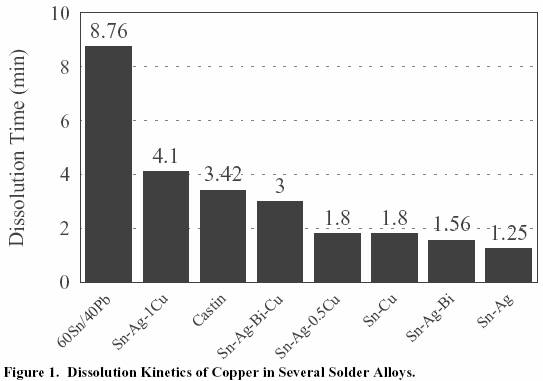
DISSOLUTION KINETICS OF COPPER
In the electronics industry, copper is commonly used as a
basis material for
• conductor traces and solder pads on the PCB
• lead frames of SO, QFP, PLCC, and other
components.
Alloys with a high tin content and a higher melting point
have a greater tendency to dissolve copper. If a larger
quantity of copper is dissolved from the base metal into
the solder material, there is excessive formation of the
Cu6Sn5 intermetallic phase. Solder joint reliability can
be adversely affected by the brittle nature of this
intermetallic compound, in
particular the mechanical
properties of the solder joint, especially under high
impact conditions.[3]
The extent of copper dissolution in various alloys can be
evaluated by means of a simple test. A 50 gram weight
was attached to a 125 µm diameter copper wire. A small
quantity of A611 liquid flux was brushed on the copper
wire. Then the alloy was placed on the tip of a soldering
iron (pre-heated to 280°C), and the soldering iron was
positioned so it made contact with the copper wire. The time
it took to break the copper wire (i.e. until the copper dissolved
in the solder) was measured and recorded as the dissolution
time.
The following alloy compositions were tested:
• 60Sn/40Pb,
• 95Sn/4Ag/1Cu,
• Castin 96.2Sn/2.5Ag/0.5Sb/0.8Cu,
• 95.5Sn/4Ag/0.5Cu,
• 88Sn/3Ag/8.5Bi/0.5Cu,
• 88.42Sn/3.07Ag/8.51Bi,
• 99.3Sn/0.7Cu,
• 96.5Sn/3.5Ag.
60Sn/40Pb had the slowest rate of dissolution of the copper
wire as expected due to its lower Sn content.
For the high tin
solders, the graph shows that the addition of 0.5% copper to
the solder alloy can decrease the dissolution rate dramatically.
In the case of the Sn/Ag/Bi alloy, the effect
of adding 0.5%Cu
was to increase the dissolution time from 1.5 minutes for
Sn/Ag/Bi to 3 minutes for Sn/Ag/Bi/0.5Cu.
8.76
4.1
3.42 3
1.8 1.8 1.56 1.25
60Sn/40Pb
Sn-Ag-1Cu
Castin
Sn-Ag-Bi-Cu
Sn-Ag-0.5Cu
Sn-Cu
Sn-Ag-Bi
Sn-Ag
0
2
4
6
8
10
Dissolution Time (min)
Figure 1. Dissolution Kinetics of Copper in Several Solder Alloys.
THE EFFECT OF ISOTHERMAL AGING
It is important to study intermetallic growth
formation
because in solder joints with coarsened Cu-Sn
intermetallics, fracture is
brittle and occurs through the
intermetallic layer. An aging
study was performed on
96.5Sn/ 3.5Ag and 95.5Sn/ 4Ag/ 0.5Cu solder alloys on
copper substrates. The intermetallic layer growth
characteristics of the two alloys were compared in order
to determine the effect of copper addition to Sn-Ag
based
alloys.
Two solder pastes were made, 96.5Sn/ 3.5Ag and
95.5Sn/ 4Ag/ 0.5Cu. The pastes were made with -325/
+500 mesh electronic grade (Type 3) powder. A 1000
gram batch of each paste was mixed in a small productionscale
Ross mixer at 89.5% metal loading/ 10.5% flux by
weight. Heraeus V365 no-clean/ halide-free flux
was used.
The test pieces were 2” x 2” copper coupons cut from 0.021
inch thick, commercial grade alloy 110 copper foil. They
were then pressed flat and cleaned in acetone. The solder
paste was screen printed through an 8 mil thick, stainless
steel, laser cut stencil on a DEK 247 printer with all printing
parameters kept constant. Therefore, the solder volume is
presumably constant and was not considered a factor in this
study. Six coupons of each alloy were printed. The printing
characteristics of both pastes were very good.
The test coupons were reflowed at Heraeus in a nitrogen
convection reflow oven using a standard profile
for the
pastes. The test pieces were then placed in a Lindberg/
Blue M air convection oven held at 150°C. The samples
were aged for periods of 2, 4, 11, 20, and 41 days (984
hours). Following aging, each sample was sectioned across 3
joints for metallographic examination. For each sample, the
average thickness of the resulting interfacial compound was
reported.
Time (hours) Intermetallic Thickness (µm)* (Cu3Sn + Cu6Sn5)
96.5Sn/ 3.5Ag 95.5Sn/
4Ag/ 0.5Cu
0 0.25 + 2 0.25 +
2
48 0.5 + 3.25 0.5 + 2.5
96 0.75 + 2.5 0.75 + 2.5
264 1 + 2.5 1 + 3
480 1.5 + 3 1.5 + 4.5
984 2.5 + 4 2.5 + **
*The standard deviation for the measurements is on the order of 0.5 µm.
**A nonuniform morphology
of the Cu6Sn5 layer precluded a characteristic thickness measurement.
It is widely known that copper is soluble in molten Sn-
Ag-X solders. The dissolution of copper results in the
formation of å-phase Cu3Sn and ç-phase Cu6Sn5. Due to
the concentration gradient, the Cu-rich Cu3Sn phase
forms adjacent to the copper substrate. Cu3Sn has a more
planar structure. The more Sn-rich Cu6Sn5 phase forms
adjacent to the Sn-based solder and has a scallop-edge
appearance. The reason why Cu6Sn5 has a scallop-edge
appearance may be due to the fact that Cu6Sn5 dissolves
faster along the grain boundary. Between the Cu6Sn5
grains, there are molten solder channels extending all the
way to the Cu3Sn/Cu interface. Since the Cu3Sn
compound layer is so thin, these channels serve as fast
diffusion and dissolution paths of Cu in the solder to feed
the interfacial reaction.[4] This interfacial layer grows
during solid-state aging as the tin and copper diffuse to
the interface and react.
The growth kinetics of the intermetallic compounds
was
found to be similar as expected due to the similar Sn
contents and reflow temperatures of the two alloys.
The
microstructural features of the
Sn-Ag-X alloys are also
similar. The matrix is polygranular Sn with a grain size
in the as-solidified condition of approximately 1 µm.[5]
Five phases can be seen in the SEM micrographs given
in Figures 6 to 17: Sn, Ag3Sn, Cu6Sn5, Cu3Sn, and Cu.
Recent work indicates that similar failure mechanisms are
involved in thermal fatigue in shear and unidirectional creep
in shear. Also, since the temperatures during thermal fatigue
represent high solder homologous temperatures, creep
deformation is involved. Creep deformation is the timedependent
plastic flow of a material under constant load at
elevated temperature. As the homologous temperature (the
ratio of the test temperature to the melting temperature on an
absolute temperature scale) increases, the ease with which
plastic flow occurs also increases. Creep is significant at a
homologous temperature greater than 0.5. Therefore, creep
deformation occurs in solders even at room temperature.
Every high temperature excursion results in a straining of the
solder joint as the constraining materials expand different
amounts. By understanding the mechanisms that lead to
fatigue failures, researchers can use the appropriate
metallurgical strategy to slow down or stop these mechanisms
and thus develop an improved, more fatigue resistant solder
alloy.[6]
The elevated operating temperature and operative strain rates
imply that creep is the major deformation mode during low
cycle fatigue. Also, the observation that solder joint fatigue
failures and creep failures appear the result of similar
metallurgical mechanisms indicates that both techniques can
be used to study the fatigue failure mechanism and relative
solder alloy fatigue resistance. As such, it becomes important
to understand how the solder microstructure accommodates
the applied strain. For the Sn-Ag-X solders,
the strain
accommodation occurs through the tin matrix at individual
Sn-Sn grain boundaries.[5]
Creep testing was performed on samples of the same
dimension and preparation method as that used for
standard tensile testing of solder alloys. All creep testing
was performed at International Tin Research Institute
(ITRI). To generate the creep-rupture data, the solder
alloys were cast into dumbbell-shaped test samples
having 20 mm gauge length and 2 mm diameter. They
were cast at a temperature of 50 degrees above the
liquidus into a heated
steel mold. The mold
was then
water cooled. Samples were then subjected to the
standard aging procedure of 24 hours at 125°C, in
addition to at least 24 hours at room temperature for the
benefit of stabilizing the microstructure as much as
possible.
Samples were held isothermally at both room
temperature and 100°C. A weight was hung from the
sample during the test representing an applied stress, and
the time to rupture was recorded. Samples and test
method conformed to the British Standard BS3500: part
3: 1969 “Method for Creep and Rupture Testing of
Metals.” Time to rupture was determined by measuring
electrical resistance across the sample; after fracture the
resistance became infinite and timing stopped. All
samples were tested in duplicate. Data was collected for
3 different loads (4, 8, and 16 MPa) at both
temperatures.
Results for time to failure at 100, 500, and 1000 hours were
recorded. Loads were applied which were expected to give
lifetimes in the region of those times but extrapolation was
carried out to estimate values for the times required. The
results at 25°C are shown in Figure 2. To interpret the data,
compare the times to rupture for a similar applied stress on
the two alloys. For example, for an applied stress of 4 MPa,
Sn/40Pb failed after 265 hours, whereas the
95.5Sn/4Ag/0.5Cu alloy took 3000 hours for failure to occur.
Figure 3 presents the data collected at ITRI for several
candidate lead free alloys compared to Sn/40Pb. The
95.5Sn/4Ag/0.5Cu alloy performs the best at room
temperature compared to Sn/3.5Ag eutectic, Sn/0.7Cu
eutectic, and Sn/40Pb. As expected, the Sn/Ag/Cu
and
Sn/Ag alloys behave similarly
due to their similar
microstructural development.
The graphic representation of
the Sn/Cu data greatly differs from that of the
other three,
perhaps indicative of a different failure mechanism. The
results of creep testing at 100°C are presented in Figure 4. At
100°C, the Sn/Ag and Sn/Ag/Cu
curves appear switched from
the 25°C results with the best performer now being the Sn/Ag
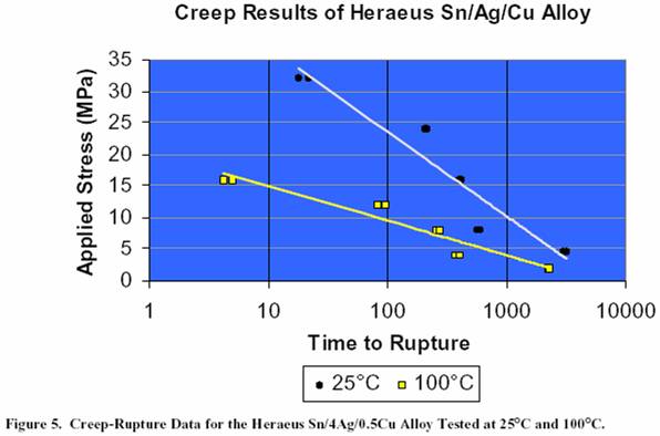
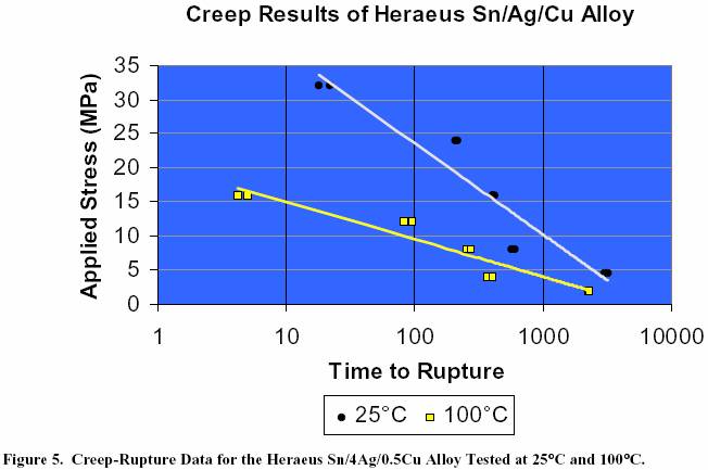
eutectic alloy. Figure 5 shows the creep-rupture data for the
Heraeus Sn/4Ag/0.5Cu
alloy tested at both room temperature
and 100°C. As expected, higher temperatures allow materials
to creep at a faster rate, thereby reducing the time to failure.
Figure 3. Creep-Rupture Data for Several Candidate Lead Free Alloys Compared
to Sn-40Pb at 25°C.
Figure 4. Creep-Rupture Data for Several Candidate Lead Free Alloys Compared
to Sn-40Pb at 100°C.
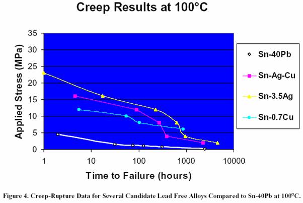
Figure 5. Creep-Rupture Data for the Heraeus
Sn/4Ag/0.5Cu Alloy Tested at 25°C and 100°C.
Recent work with candidate lead free alloys indicate a
significant improvement in reliability over Sn/Pb.
Figures 2-4 clearly demonstrate a superior creep
resistance over Sn/Pb for all lead free alloys
tested
including Sn/Ag eutectic, Sn/Cu
eutectic, and
Sn/4Ag/0.5Cu at both room temperature and 100°C.
Although the Sn/Cu eutectic outperformed Sn/40Pb,
it
did not perform as well as the Sn-Ag-X alloys.
An aging study of both the 95.5Sn/4Ag/0.5Cu and
96.5Sn/3.5Ag solder alloys was performed in order to
evaluate the growth kinetics of the intermetallic
layers
following extended heat treatment. An understanding of
the microstructural evolution that occurs at
the
solder/copper interface at elevated temperatures is helpful
to understand the failure mechanisms that dominate at
elevated temperatures. Creep occurs when materials
under constant stress, below the tensile stress, slowly
deform and finally fracture. The creep rate is dependent
on alloy composition and microstructure and is strongly
temperature dependent. Because Sn/Ag and Sn/Ag/Cu
have similar microstructures, they behave similarly
during isothermal aging and creep testing.
The author is grateful to acknowledge the support of the
International Tin Research Institute for mechanical
testing of the alloys. The metallographic preparation and
scanning electron microscopy of the samples used to study
aging was performed by F.W. Gayle and L. Smith at the
National
appreciated. Also, thanks to Dr. M.R. Notis of
Lehigh
University and A. Z. Miric of Heraeus
useful discussions.
1.
Solder Project Final Report, August 1997.
2. P.T. Vianco, K.L. Erickson,
and P.L. Hopkins, “Solid
State Intermetallic Compound Growth Between Copper
and High Temperature, Tin-Rich Solders-Part I:
Experimental Analysis,” Sandia National Labs
(Contract
Number DE-AC04-94AL85000), 1994.
3. G. Humpston and D.M. Jacobson,
Principles of Soldering
and Brazing, ASM International,
1993.
4. H.K. Kim and K.N. Tu, “Kinetic
Analysis of the
Soldering Reaction Between Eutectic SnPb Alloy
and Cu
Accompanied by Ripening,” Physical Review B, Vol. 53,
No. 23,
5. D.R. Frear, “The Mechanical
Behavior of Interconnect
Materials for Electronic Packaging,” J.Metals,
(May
1996), pp. 49-53.
6. J.W. Morris, Jr. and D.
Tribula, “Creep in Shear of
Experimental Solder Joints,” Journal of Electronic
Packaging, June 1990, Vol.
112, pp. 87-93.
Integrity of Solder Joints from Lead-free Solder Paste
Angela Grusd
Heraeus Inc.
West Conshohocken, PA
This past year the Lead Free
Movement has taken center stage in the electronics
assembly industry. In
December 1997, the Japan Environmental
Agency proposed legislation on the disposal of lead scrap. Leadcontaining
scrap, such as electronics,
must be disposed of in sealed landfill sites to prevent the leaching
of lead.
A second Japanese proposal
was initiated by the Ministry of International Trade and Industry
(MITI) and the
(excluding batteries) by 2001
and a 66.67% reduction by 2003. The committee of JEIDA (Japan Electronic
Industry Development Association)
and the lead-free soldering committee of JIEP (Japan Institute of
Electronics
Packaging) outlined the lead-free
road map for soldering on
major Japanese Consumer Electronic
Manufacturers initiated their own road map and publicly announced
accelerated plans to eliminate
lead solder completely by 2001.
Matsushita (Panasonic):
It is reported that by 2001,
all lead will be eliminated from major electronics products. Since
compact mini-disc player has
been available in
contains a Sn/Ag/Bi/Cu lead free solder. The product is about half the
size of a compact disc player, kind of a
portable walkman. In March
of 1999, this product will be launched in
lead free solder can be achieved
such that no problems regarding material properties, installaiton quality, and
reliability arise in actual
production and implementation is being proceeded to meet their 2001
target.
Following this product, Matsushita
will introduce lead free audio stereos, car stereos, and televisions
into
at the beginning of 1999 and
in
affected and advised to change
to lead free by
industry in the
Sony:
By 2001, all lead will be
eliminated except for high density electronics packaging.
Toshiba:
By 2000, lead will be eliminated
from mobile phones.
By 1999, lead usage reduced
to half of that in 1997. By 2001, all products will be lead-free.
In April,1998 the Japanese
started a project similar to the
Project called the NEDO project.
The project goal is to make a data base on lead-free soldering, to
select leadfree
solders, and to establish
the process for lead-free solders. The total budget is 350,000,000
yen/two years.
Project members are from major
electronics companies, device companies, solder companies, and several
universities.
Another important alloy is
the Sn/Ag/Cu system. Sn/Ag/Cu
is also on the list of the JEIDA lead free roadmap.
In addition, the European
Brite-Euram Consortia recommended Sn/Ag/Cu
as the general purpose solder. The
Sn-Ag-X lead free solders offer
superior creep resistance at room temperature and 100°C as compared to Sn-
40Pb. Results of this work
will be presented as well as factors to consider when developing and
implementing
lead free alloys such as manufacturability,
availability, and cost. One of the most promising replacement alloys
is Sn/4Ag/0.5Cu. This alloy
will be discussed in detail.
Lead free alternatives are
being considered for several reasons:
• Health Concerns
It is widely known that lead
is related to certain health risks. If lead particles are inhaled
or ingested, they
accumulate in the human body
causing damage to the blood and central nervous systems. Lead poisoning
can be
detected by blood analysis
and the limits are defined by national governments. The standard upper
value of
untainted human beings should
not exceed 130 µg/l. The upper blood lead limit of people who are
exposed to
lead at work is, according
to the
300 µg/l blood for women and
700 µg/l for men. In the
to 100 µg/l.
As a result, some industries
have already eliminated lead and have found suitable alternatives,
for example
plumbing solders, tinned cans,
lead-free gasoline for vehicles, and lead-free cut crystal glass.
The majority of
lead consumption is automobile
batteries and ammunition. The lead consumption of the electronics
industry is
relatively small and, according
to different sources, lies between 0.5 - 7%.
When choosing alternative
metals, consideration must also be given to their health risks as
well. Recent studies
in the
alternative metals:[1]
• Cd is extremely toxic and should
not be used (high risk). Many companies such as Ford Motor Company
have banned Cd-containing materials.
• Pb was also identified as highly
toxic (high risk - it is considered harmful to the reproductive system).
• Sb is very toxic and should
not be considered a major alloying element (medium risk - in Europe
this
material is considered potentially
carcinogenic).
• Ag and Cu are used in lead-free
alloys in small concentrations - in Europe these materials are seen
as low
risk.
• Sn and Zn are essential elements
in the human diet, yet may be toxic if exposures are sufficiently
high (low
risk).
• Bi is a relatively benign
metal with a history of medicinal uses (low risk).
• Greater Thermal Stress of Components
In the automotive industry,
more and more circuits are being placed in the engine compartment
in order to
reduce the quantity of cables
and, therefore, reduce cost. These under the hood conditions often
see
temperatures in excess of
150°C. A leading automobile manufacturer has even measured temperatures
as high
as 170°C on a hybrid circuit.
The high thermal stresses imposed on the solder joints at these temperatures
has
led automotive manufacturers
to research Pb-free alternatives with high
thermal fatigue resistance, because they
observed that Sn-37Pb has
poor thermal fatigue properties even at 125°C. Higher temperatures
dramatically
reduce the strength of the
solder joint during thermal cycling, due to greater plastic deformation
of the solder as
well as diffusion, recrystallization and grain growth inside the solder.
For conventional alloys such
as Sn62/Pb36/Ag2 (melting point 179°C) and Sn63/Pb37 (melting point
183°C),
there is a major concern for
the mechanical and microstructural stability
and, therefore, the reliability of the
solder joint at an operating
temperature of 150°C, because it is approaching
the melting point of the alloy.
LEAD FREE ALTERNATIVE SOLDER ALLOYS
96.5Sn/3.5Ag
221°C
This alloy exhibits adequate
wetting behavior and strength and is used
in electronics as well as plumbing.
Several sources have also
reported good thermal fatigue properties as compared to Sn/Pb.
Thermal fatigue
damage in solders is accelerated
at elevated temperatures. In the Sn/Pb system,
the relatively high solid
solubilities of Pb
in Sn and vice versa, especially at elevated
temperatures, lead to microstructural instability
due
to coarsening mechanisms.
These regions of inhomogeneous microstructural
coarsening are known to be crack
initiation sites. It is well-documented
that these types of microstructures in Sn/Pb
alloys fail by the formation of
a coarsened band in which
a fatigue crack grows. By comparison, the Sn/Ag
system, has limited solid solubility
of Ag in Sn, making it more resistant to coarsening. As a result, Sn/3.5Ag
eutectic forms a more stable, uniform
microstructure that is more
reliable.
Although the Sn/3.5Ag alloy
itself exhibits good microstructural stability,
when soldered to copper base metal,
the combination of a higher
Sn content (96.5Sn compared to 63Sn) and
higher reflow temperature environments
accelerate the diffusion rates
for copper base metal in Sn. As its corresponding
composition is reached, the
brittle Cu6Sn5 intermetallic compound is nucleated and
begins to grow. To slow the diffusion rate and thereby
decrease the growth kinetics,
alternative surface finishes such as immersion gold (Au over Ni over
Cu) may be
used. The 2 µm Ni in the immersion gold
coating serves as an effective diffusion barrier, limiting the Cu
from
diffusing into the solder
and forming the brittle Cu6Sn5 intermetallic compound. Other surface finishes
such as
immersion silver (Ag over
Cu) and immersion palladium (Pd over Cu) do not contain a Ni barrier
layer. Their
effect on the growth kinetics
of the intermetallic compound layers is
under investigation.
95.5Sn/4.0Ag/0.5Cu 217-219°C
Because the mechanical stability
of the joint is degraded when the melting point is approached, elevated
temperature cycling produces
more damage for Sn/Pb solder (m.p. 183°C) as compared to higher melting point
solders. The melting temperatures
of Sn/Ag/Cu solders make them ideal in high
operating temperatures up to
175°C. As for wetting, Sn/Ag/Cu solders do not wet Cu as well as Sn/Pb using commercial fluxes. However,
good fillet formation can
be easily achieved provided the fluxes are suitable for higher temperature
use.
Soldering in nitrogen atmosphere
also improves wettability using no-clean
fluxes. The copper dissolution test
provides a relative measurement
of the solder’s tendency to dissolve Cu from the base metal and form
the
Cu6Sn5 intermetallic compound.
99.3Sn/0.7Cu 227 °C
This alloy might be also suitable
for high temperature applications required by the automotive industry.
It is a
candidate especially for companies
looking for lead and silver free alloys. Preliminary testing conducted
on this
alloy has shown a significant
improvement in creep/fatigue data over standard Sn-Pb
alloys. However, the Sn-
Ag-X alloys perform better
in creep testing.
96.2Sn/2.5Ag/0.8Cu/0.5Sb (known as Castin) 217-220 °C
This alloy has similar mechanical
properties and reliability characteristics to the Sn/Ag/Cu alloy. However,
there is some concern regarding
the toxicity of Sb.
91.8Sn/3.4Ag/4.8Bi 200-216°C
In general, bismuth is added
to Sn/Ag/X solder alloys in order to depress
the melting point. Another benefit of
Bi addition is greater joint
strength as indicated by ring and plug testing. This particular alloy
was developed by
Sandia National Labs. Sandia’s internal studies have found no electrical failures
on surface mount devices
following 10,000 thermal cycles
using 68 I/O PLCCs, 24 I/O SOICs,
and 1206 chip capacitors on standard FR-4
PCBs. The boards were cycled
0 to 100°C at a ramp rate of 10°C/ minute. No cracks or deformation
were
observed on boards cross-sectioned
after 5000 thermal cycles. Cross-sectional data on 10,000 cycles is
being
collected. These results are
in good agreement with data collected by the
Sciences (NCMS) Lead Free
Solder Project, which reported very good thermal fatigue resistance
on OSP
printed circuit boards (Organic
Solderability Preservative that protects
copper pads and through-holes). The
NCMS High Temperature Fatigue
Resistance Project is currently evaluating this solder at temperatures
up to
160 and 175°C. In combination
with Pb from the PCB or component metallization,
a Sn/Bi/Pb ternary
compound is formed with a
melting point of only 96°C. As the trend toward eliminating lead continues,
this
alloy may become more attractive.
90Sn/2.0Ag/7.5Bi/0.5Cu (138) 198-212°C
Although the addition of Bi
to the Sn/Ag/X system imparts greater strength
and improved wetting, too much
bismuth (greater than 5%)
leads to the presence of a small DSC peak near 138°C, corresponding
to the binary
Sn/Bi eutectic at 138°C or the
ternary Sn/Ag/Bi eutectic at 136.5°C. For
this alloy with 7.5 weight percent Bi,
this corresponds to approximately
1% of the total melting. This small amount of eutectic melting has
an
uncertain effect on joint
reliability as the temperature approaches 138°C. This combined with
the
aforementioned concern of
forming a SnPbBi compound at 96°C, makes
this alloy an unlikely candidate for a
Pb-free solder.
42Sn/58Bi 138°C
The low melting point of this
alloy makes it suitable for soldering temperature-sensitive components
and
substrates. If these contain
Pb, the SnPbBi
ternary eutectic compound may form at 96°C, which in turn adversely
affects the thermal fatigue
properties. The NCMS Lead Free Solder Project recently reported the
results of
thermal cycle testing at 0/
100°C and -55/ +125°C for over 5000 cycles on OSP boards. The result
was that the
Sn/Bi outperformed the Sn/Pb at both temperature excursions. It was thought that
the closeness of 125°C to the
binary Sn/Bi
eutectic at 138°C would cause this alloy to be a poor performer. Two
possible explanations for this
unexpected result were presented.
The Sn/Bi alloy may be annealing at 125°C,
relaxing the stresses produced
during thermal cycling. A
second explanation was the alloy may be undergoing recrystallization.
Also, no filletlifting
was observed due to the eutectic
nature of the alloy.
95Sn/5Sb 232-240°C
The 95Sn-5Sb solder is a solid
solution of antimony in a tin matrix. The relatively high melting
point of this
alloy makes it suitable for
high temperature applications. The antimony imparts strength and hardness.
In
comparing the yield strengths
of several solder alloys, the strength of 95Sn/5Sb was 37.2 N/mm2 and was nearly
the same as 96.5Sn/3.5Ag (37.7
N/mm2 ).[2] The high strength of this
alloy causes the lowest energy crack path
to be at the solder/intermetallic interface in the case of thinner intermetallics. As the intermetallic
thickens, the
crack path is through the
intermetallic layer. Formation of the intermetallic
compound SbSn is possible at these
levels of Sb. This phase has a cubic structure with a high hardness.
The wetting behavior was measured on a
wetting balance in air using
a standard RMA flux. The wetting force at 2 seconds for 95Sn/5Sb on
a Cu wire is
significantly less than Sn/37Pb
and Sn/3.5Ag. In addition to marginal wetting performance, the toxicity
of Sb
has also raised concerns.
As with bismuth, antimony is also a by-product in the production of
lead.
In/Sn
52In/48Sn 118°C
The melting point of this
alloy makes it suitable to low temperature applications. With regard
to indium, it
displays good oxidation resistance,
but is susceptible to corrosion in a humid environment. It is also
a very soft
metal and has a tendency to
cold weld. In addition, the 52In/48Sn alloy displays rather poor high
temperature
fatigue behavior,
due to its low melting point. The high indium content limits the widespread
use of this alloy
due to cost and availability
constraints.
91Sn/9Zn 199°C
The presence of zinc in solder
alloys leads to oxidation and corrosion. Samples of bulk alloys that
were steam
aged for 8 hours exhibited
severe corrosion as evidenced by a purplish color.
In powder form, it reacts rapidly
with acids and alkalis and
forms a gas. Zinc-containing solder alloys have been known to react
with the flux
medium in as little as a day,
resulting in a paste that is “hard as a rock”. Thus, its compatibility
with fluxes and
its storage stability is questionable.
The reflowed solder joints do not wet as
well as other lead-free alloys.
When wave soldered, this alloy
tends to produce excessive dross. Therefore, manufacturability of
this alloy and
zinc-bearing alloys in general
is a concern.
Au/Sn
80Sn/20Au 280°C
Au/Sn
eutectic solder is a very strong, rigid solder due to the formation
of brittle intermetallic compounds.
Problems of cracked dies have
been seen using Au/Sn eutectic solders in
die attach applications. It is not known
if the cracks occur from processing
or during thermal cycling. The high cost of this alloy restricts its
use in
many applications where cost
is a factor.
DISSOLUTION KINETICS OF COPPER
In the electronics industry,
copper is commonly used as a basis material for
• conductor traces and solder
pads on the PCB
• lead frames of SO, QFP, PLCC,
and other components.
Alloys with a high tin content
and a higher melting point have a greater tendency to dissolve copper.
If a larger
quantity of copper is dissolved
from the base metal into the solder material, there is excessive formation
of the
Cu6Sn5 intermetallic phase. Solder joint reliability
can be adversely affected by the brittle nature of this
intermetallic compound, in particular the
mechanical properties of the solder joint, especially under high impact
conditions.[3]
The extent of copper dissolution
in various alloys can be evaluated by means of a simple test. A 50
gram weight
was attached to a 125 µm diameter
copper wire. A small quantity of A611 liquid flux was brushed on the
copper
wire. Then the alloy was placed
on the tip of a soldering iron (pre-heated to 280°C), and the soldering
iron was
positioned so it made contact
with the copper wire. The time it took to break the copper wire (i.e.
until the
copper dissolved in the solder)
was measured and recorded as the dissolution time.
The following alloy compositions
were tested: 60Sn/40Pb, 95Sn/4Ag/1Cu, Castin
96.2Sn/2.5Ag/0.5Sb/0.8Cu,
95.5Sn/4Ag/0.5Cu, 88Sn/3Ag/8.5Bi/0.5Cu, 88.42Sn/3.07Ag/8.51Bi,
99.3Sn/0.7Cu, and 96.5Sn/3.5Ag.
60Sn/40Pb had the slowest
rate of dissolution of the copper wire as expected due to its lower
Sn content. For
the high tin solders, the
graph shows that the addition of 0.5% copper to the solder alloy can
decrease the
dissolution rate dramatically.
In the case of the Sn/Ag/Bi alloy, the effect
of adding 0.5%Cu was to increase the
dissolution time from 1.5
minutes for Sn/Ag/Bi to 3 minutes for Sn/Ag/Bi/0.5Cu.
Figure 1. Dissolution Kinetics
of Copper in Several Solder Alloys.
THE EFFECT OF ISOTHERMAL AGING
It is important to study intermetallic growth formation because in solder joints with
coarsened Cu-Sn
intermetallics, fracture is brittle and
occurs through the intermetallic layer.
An aging study was performed on
96.5Sn/ 3.5Ag and 95.5Sn/
4Ag/ 0.5Cu solder alloys on copper substrates. The intermetallic
layer growth
characteristics of the two
alloys were compared in order to determine the effect of copper addition
to Sn-Ag
based alloys.
Two solder pastes were made,
96.5Sn/ 3.5Ag and 95.5Sn/ 4Ag/ 0.5Cu. The pastes were made with -325/
+500
mesh electronic grade (Type
3) powder. A 1000 gram batch of each paste was mixed in a small productionscale
Ross mixer at 89.5% metal
loading/ 10.5% flux by weight. Heraeus V365
no-clean/ halide-free flux was
used.
The test pieces were 2” x
2” copper coupons cut from 0.021 inch thick, commercial grade alloy
110 copper foil.
They were then pressed flat
and cleaned in acetone. The solder paste was screen printed through
an 8 mil thick,
stainless steel, laser cut
stencil on a DEK 247 printer with all printing parameters kept constant.
Therefore, the
solder volume is presumably
constant and was not considered a factor in this study. Six coupons
of each alloy
were printed. The printing
characteristics of both pastes were very good.
The test coupons were reflowed at Heraeus in a nitrogen
convection reflow oven using a standard
profile for the
pastes. The test pieces were
then placed in a Lindberg/ Blue M air convection oven held at 150°C. The samples
were aged for periods of 2,
4, 11, 20, and 41 days (984 hours). Following aging, each sample was
sectioned
across 3 joints for metallographic
examination. For each sample, the average thickness of the resulting
interfacial compound was reported.
Time (hours) Intermetallic Thickness (µm)* (Cu3Sn + Cu6Sn5)
96.5Sn/ 3.5Ag 95.5Sn/ 4Ag/ 0.5Cu
0 0.25 + 2 0.25 + 2
48 0.5 + 3.25 0.5 + 2.5
96 0.75 + 2.5 0.75 + 2.5
264 1 + 2.5 1 + 3
480 1.5 + 3 1.5 + 4.5
984 2.5 + 4 2.5 + **
*The standard deviation for
the measurements is on the order of 0.5 µm.
**A nonuniform
morphology of the Cu6Sn5 layer precluded a characteristic
thickness measurement.
It is widely known that copper
is soluble in molten Sn-Ag-X solders. The
dissolution of copper results in the
formation of å-phase Cu3Sn and ç-phase Cu6Sn5. Due to the concentration
gradient, the Cu-rich Cu3Sn phase
forms adjacent to the copper
substrate. Cu3Sn has a more
planar structure. The more Sn-rich Cu6Sn5 phase
forms adjacent to the Sn-based solder and has a scallop-edge appearance. The reason
why Cu6Sn5 has a scallopedge
appearance may be due to the
fact that Cu6Sn5 dissolves faster along the
grain boundary. Between the
Cu6Sn5 grains, there are molten solder
channels extending all the way to the Cu3Sn/Cu interface. Since the
Cu3Sn compound layer is so thin,
these channels serve as fast diffusion and dissolution paths of Cu
in the solder
to feed the interfacial reaction.[4] This interfacial layer grows
during solid-state aging as the tin and copper
diffuse to the interface and
react.
The growth kinetics of the
intermetallic compounds was found to be similar as expected
due to the similar Sn
contents and reflow temperatures of the two alloys. The microstructural features of the Sn-Ag-X
alloys are also
similar. The matrix is polygranular Sn with a grain size
in the as-solidified condition of approximately 1 µm.[5]
Five phases were identified
in the SEM micrographs: Sn, Ag3Sn, Cu6Sn5, Cu3Sn, and Cu.
Recent work indicates that
similar failure mechanisms are involved in thermal fatigue in shear
and unidirectional
creep in shear. Also, since
the temperatures during thermal fatigue represent high solder homologous
temperatures, creep deformation
is involved. Creep deformation is the time-dependent plastic flow
of a material
under constant load at elevated
temperature. As the homologous temperature (the ratio of the test
temperature to
the melting temperature on
an absolute temperature scale) increases, the ease with which plastic
flow occurs also
increases. Creep is significant
at a homologous temperature greater than 0.5. Therefore, creep deformation
occurs in solders even at
room temperature. Every high temperature excursion results in a straining
of the solder
joint as the constraining
materials expand different amounts. By understanding the mechanisms
that lead to
fatigue failures, researchers
can use the appropriate metallurgical strategy to slow down or stop
these
mechanisms and thus develop
an improved, more fatigue resistant solder alloy.[6]
The elevated operating temperature
and operative strain rates imply that creep is the major deformation
mode
during low cycle fatigue.
Also, the observation that solder joint fatigue failures and creep
failures appear the
result of similar metallurgical
mechanisms indicates that both techniques can be used to study the
fatigue failure
mechanism and relative solder
alloy fatigue resistance. As such, it becomes important to understand
how the
solder microstructure accommodates
the applied strain. For the Sn-Ag-X solders,
the strain accommodation
occurs through the tin matrix
at individual Sn-Sn grain boundaries.[5]
Creep testing was performed
on samples of the same dimension and preparation method as that used
for
standard tensile testing of
solder alloys. All creep testing was performed at International Tin
Research Institute
(ITRI). To generate the creep-rupture
data, the solder alloys were cast into dumbbell-shaped test samples
having 20 mm gauge length
and 2 mm diameter. They were cast at a temperature of 50 degrees above
the
liquidus into a heated steel mold. The mold was then water cooled.
Samples were then subjected to the
standard aging procedure of
24 hours at 125°C, in addition to at least
24 hours at room temperature for the
benefit of stabilizing the
microstructure as much as possible.
Samples were held isothermally
at both room temperature and 100°C. A weight was
hung from the sample
during the test representing
an applied stress, and the time to rupture was recorded. Samples and
test method
conformed to the British Standard
BS3500: part 3: 1969 “Method for Creep and Rupture Testing of Metals.”
Time to rupture was determined
by measuring electrical resistance across the sample; after fracture
the
resistance became infinite
and timing stopped. All samples were tested in duplicate. Data was
collected for 3
different loads (4, 8, and
16 MPa) at both temperatures. Results for
time to failure at 100, 500, and 1000 hours
were recorded. Loads were
applied which were expected to give lifetimes in the region of those
times but
extrapolation was carried
out to estimate values for the times required. The results at 25°C are shown in Figure
2. To interpret the data,
compare the times to rupture for a similar applied stress on the two
alloys. For
example, for an applied stress
of 4 MPa, Sn/40Pb failed after 265 hours,
whereas the 95.5Sn/4Ag/0.5Cu alloy
took 3000 hours for failure
to occur.
Figure 3 presents the data
collected at ITRI for several candidate lead free alloys compared
to Sn/40Pb. The
95.5Sn/4Ag/0.5Cu alloy performs
the best at room temperature compared to Sn/3.5Ag eutectic, Sn/0.7Cu
eutectic, and Sn/40Pb. As
expected, the Sn/Ag/Cu and Sn/Ag
alloys behave similarly due to their similar
microstructural development. The graphic
representation of the Sn/Cu data greatly
differs from that of the other
three, perhaps indicative
of a different failure mechanism. The results of creep testing at
100°C are presented in
Figure 4. At 100°C, the Sn/Ag and Sn/Ag/Cu curves appear switched from the 25°C results with the best
performer now being the Sn/Ag eutectic alloy. Figure 5 shows the creep-rupture data
for the Heraeus
Sn/4Ag/0.5Cu alloy tested
at both room temperature and 100°C. As expected, higher temperatures
allow
materials to creep at a faster
rate, thereby reducing the time to failure.
Figure 2. Creep-Rupture Data
for Heraeus Sn-4Ag-0.5Cu and Sn-40Pb at
25°C.
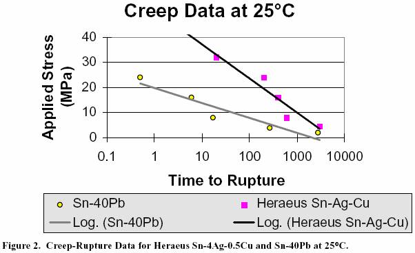
Figure 3. Creep-Rupture Data
for Several Candidate Lead Free Alloys Compared to Sn-40Pb at 25°C.
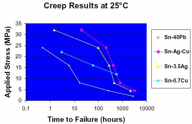
Figure 4. Creep-Rupture Data
for Several Candidate Lead Free Alloys Compared to Sn-40Pb at 100°C.
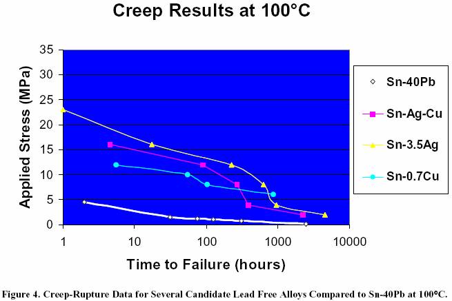
Figure 5. Creep-Rupture Data
for the Heraeus Sn/4Ag/0.5Cu Alloy Tested
at 25°C and 100°C.
This first lesson appears
too easy and is often overlooked. When testing Bi-containing lead
free alloys, many
companies have had to scrap
many hours worth of otherwise valuable data because they used the
standard Sn/Pb
component finish or PWB board
metallization. As reported earlier, in combination with Pb from the PWB or
component metallization, a
Sn/Bi/Pb ternary compound is formed with a melting point of
only 96°C. These
joints would not be able to
undergo thermal cycling and are technically unsalvageable.
This second valuable lesson
is not so obvious and was discovered by the NCMS High Temperature
Fatigue
Resistant Solder Project Team.
Components used for the PWB and hybrid assemblies for the
Thermomechanical Fatigue Test build had leads
or castellations, in the case of the LCCCs, pretinned with pure
tin. The large volume of Sn on the leads and castellations
resulted in a contamination of the final solder joints.
The problem was initially
identified in the case of the high lead alloys because they melted
at the eutectic
temperature of 183°C and had the eutectic Sn/Pb
morphology. The problem was less severe in the Sn-based
lead free alloys but still
a major problem. With the LCC 44 component, a 50% dilution of the
alloys was
reported. The Sn contamination for the PLCCs was
far less as expected, since the “tinning” volume is much
less, with only a 15 -20 micron
thick coating on the leads. A 10% dilution was reported for the PLCC
components. The selected alloys
were far enough from their targeted compositions that the NCMS Team
chose
to repeat the entire assembly.
In the future work of the project, components will not be supplied
with pure tin or
tin-lead solder. The preferred
alternative is to prealloy the components
with the test alloys to avoid
contamination.
Recent work with candidate
lead free alloys indicate a significant improvement in reliability
over Sn/Pb.
Figures 2-4 clearly demonstrate
a superior creep resistance over Sn/Pb for
all lead free alloys tested including
Sn/Ag eutectic, Sn/Cu eutectic, and Sn/4Ag/0.5Cu at both room temperature
and 100°C. Although the Sn/Cu
eutectic outperformed Sn/40Pb,
it did not perform as well as the Sn-Ag-X
alloys.
An aging study of both the
95.5Sn/4Ag/0.5Cu and 96.5Sn/3.5Ag solder alloys was performed in order
to
evaluate the growth kinetics
of the intermetallic layers following extended
heat treatment. An understanding of
the microstructural
evolution that occurs at the solder/copper interface at elevated temperatures
is helpful to
understand the failure mechanisms
that dominate at elevated temperatures. Creep occurs when materials
under
constant stress, below the
tensile stress, slowly deform and finally fracture. The creep rate
is dependent on alloy
composition and microstructure
and is strongly temperature dependent. Because Sn/Ag and Sn/Ag/Cu have
similar microstructures, they
behave similarly during isothermal aging and creep testing.
The author is grateful to
acknowledge the support of the International Tin Research Institute
for mechanical
testing of the alloys. The
metallographic preparation and scanning electron microscopy of the
samples used to
study aging was performed
by F.W. Gayle and L. Smith at the National Institute of Standards
and Technology
and is greatly appreciated.
Also, thanks to Dr. M.R. Notis of
1.
2. P.T. Vianco, K.L. Erickson,
and P.L. Hopkins, “
Copper and High Temperature,
Tin-Rich Solders-Part I: Experimental Analysis,” Sandia National Labs
(Contract Number DE-AC04-94AL85000),
1994.
3. G. Humpston and D.M. Jacobson,
Principles of
Soldering and Brazing, ASM International, 1993.
4. H.K. Kim and K.N. Tu, “Kinetic
Analysis of the Soldering Reaction Between Eutectic SnPb Alloy and Cu
Accompanied by Ripening,”
Physical Review B, Vol. 53, No. 23,
5. D.R. Frear, “The Mechanical
Behavior of Interconnect Materials for Electronic
Packaging,” J.Metals, (May
1996), pp. 49-53.
6. J.W. Morris, Jr. and D.
Tribula, “Creep in Shear of Experimental Solder Joints,” Journal of Electronic
Packaging, June 1990, Vol. 112, pp. 87-93.
Previously published
in German in
Productronic,
11/97.
©Productronic,
1997
Anton
Zoran Miric
W.C.
Heraeus GmbH,
Angela
Grusd
Heraeus
Cermalloy Division, West
[ 19
]
In recent years, efforts
to develop alternatives to leadbased solders
have increased dramatically. These efforts began as a response to
potential legislation and regulations restricting lead usage in the
electronics industry. Lead is extremely toxic when inhaled or ingested.
As researchers began to focus on Pb-free
solders, they recognized their value in high temperature applications
(e.g. automotive manufacturing) where Sn/Pb solders do not meet the requirements.
There are many factors
to consider when developing lead-free alloys: manufacturability, availability,
reliability, cost and environmental safety. Of these, the most challenging
and time consuming is the reliability of alternative solders. The
lead-free alloys available cannot be used as a drop-in replacement
for the SnPb or SnPbAg.
The introduction of lead-free solder alloys may mean having to use
alternative component and PCB metallizations,
PCB materials, solder fluxes, etc.
Lead is
used in the electronics industry as a part of the solder material
alloy. For some time, now, alternative materials have been called
for, for several reasons.
Greater thermal stress
of components
In the
automotive industry, more and more circuits are being
• greater
plastic deformation of the solder;
• recrystallisation and grain growth inside the solder.
At such
high temperatures, the mechanical properties of the
service
temperature is c. 97 per cent of the melting temperature
Minimisation of health
risks
The use
of lead alloys is related to certain health risks, e.g.
If chronically
exposed to lead, an accumulation of lead in
In the
manufacturing environment, lead constitutes only a
A greater
danger lies in the contamination of ground
Several
proposals have been made to limit, tax or ban the
Nevertheless,
one has to remember that the major part of
The lead
consumption of the electronics industry is
When choosing
alternative metals, consideration must
• Cd is extremely toxic and should not be used (high risk).
• Pb was also identified as highly toxic (high risk – in
• Sb is very toxic and should not be considered a major
• Ag and
Cu are used in lead-free alloys in small concentrations
• Sn and Zn are essential elements in the human diet, yet
• Bi is
a relatively benign metal with a history of medicinal
Use of temperature-sensitive
components and
Many industries
strive to reduce costs. Components and
This is
especially apparent with consumer electronics, as
2. Alternative materials and solder
alloys
Some alternative
basis metals and their alloys are shown in
Sn/Ag: 96.5Sn/3.5Ag; 221°C
This alloy
exhibits adequate wetting behaviour and strength
Several
sources have also reported good thermal fatigue
These regions
of inhomogeneous microstructural coarsening
Although
the Sn-3.5Ag alloy itself exhibits good
Technology
|
|
|||||||||||||||||||||||||||||
|
|
|||||||||||||||||||||||||||||
|
|
|||||||||||||||||||||||||||||
|
|||||||||||||||||||||||||||||
|
|
|||||||||||||||||||||||||||||
|
|
10/1 [1998]
19–25
Anton Zoran Miric and
Anton Zoran Miric and
The Ni
in the immersion gold coating serves as a diffusion
surface
finishes such as immersion silver (Ag over Cu) and
Sn/Ag/Cu
1 95.5Sn/4.0Ag/0.5Cu; 216-219°C
2 95.5Sn/3.8Ag/0.7Cu; 217-219°C
3 95.0Sn/4.0Ag/1.0Cu; 216-219°C
4 93.6Sn/4.7Ag/1.7Cu;
216-218°C
Because
the mechanical stability of the joint is degraded
point 183°C)
as compared to higher melting point solders.
The melting
temperatures of Sn-Ag-Cu solders make them
using commercial
fluxes. However, improved wetting is
Sn/Cu:
99.3Sn/0.7Cu; 227°C
This alloy
might be also suitable for high temperature
Sn/Ag/Cu/Sb: 96.7Sn/2Ag/0.8Cu/0.5Sb
(known as Castin-Alloy); 217-220°C
This alloy
has similar properties to the Sn/Ag/Cu alloy.
Sn/Ag/Bi: 91.8Sn/3.4Ag/4.8Bi;
200-216°C
In general,
bismuth is added to Sn-Ag-X solder alloys
in
In combination
with Pb from the PCB or component
Sn/Ag/Bi/Cu: 90Sn/2.0Ag/7.5Bi/0.5Cu;
(138) 198-212°C
Although
the addition of Bi to the Sn-Ag-X system
imparts
Sn/Bi:
42Sn/58Bi; 138°C
The low
melting point of this alloy makes it suitable for
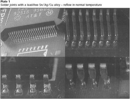
Solder joints with a
lead-free Sn/Ag/Cu alloy – reflow
in nitrogen
Solder joints with a
lead-free Sn/Ag/Cu alloy – reflow
in normal temperature
Anton Zoran Miric and
The NCMS
Lead Free Solder Project recently reported
From a
raw material perspective, bismuth is a by-product
Sn/Sb:
95Sn/5Sb; 232-240°C
The relatively
high melting point of this alloy makes it
suitable
for high temperature applications. The antimony
has the
effect of imparting strength and hardness to the
alloy.
Formation of the intermetallic compound
SbSn is
possible
at these levels of Sb. This phase has a
cubic structure
with a
high hardness. The wetting behaviour was
measured
on a wetting balance in air using a standard RMA
flux. The
wetting force at two seconds for 95Sn/5Sb on a Cu
wire is
significantly less than Sn/37Pb and Sn/3.5Ag. In
addition
to marginal wetting performance, the toxicity of Sb
has also
raised concerns. One source reported that with
more than
4 per cent antimony in the alloy the tensile
strength
is reduced and the joints have a variable and occasionally
low fatigue
strength. As with Bi, antimony is also a
by-product
in the production of lead.
Sn/Ag/Sb:
65Sn/25Ag/10Sb (known as
Motorola J Alloy); 230-235°C
Motorola
J alloy is a relatively high temperature alloy that
displays
good creep resistance. Most notably, this alloy is
currently
used as a replacement for Au-Si die attach
material.
One company
that uses Motorola J has expressed concern
that the
alloy may be too strong and sometimes breaks
the die.
This behaviour can be explained in terms of the
alloy microstructure
and resulting properties. With this
relatively
high amount of antimony, a large amount of the
hard SbSn phase is likely present. These SbSn
cubes can act
as crack
initiation sites and eventually lead to failures.
Therefore,
the high strength which the high antimony
content
imparts may prove to be too stiff for microelectronics
applications
where compliance to shear stresses is a
requirement.
The large
amount of Sb may also be responsible for
the
very poor
wetting behaviour of Motorola J alloy. Wetting
balance
measurements taken in air using a standard RMA
flux show
that the force at two seconds is considerably less
than Sn/37Pb,
Sn/3.5Ag, and even 95Sn/5Sb, which is
known to
be marginal/difficult in circuit assembly. The
rapid oxidation
of antimony is likely a factor. Another
source
reported that the poor wetting behaviour was due to a
Ag content
of >4 per cent, due to a decreased fluidity. This
observation
can be attributed to the formation of a substantial
amount
of the needle-like Ag3Sn phase which is solid
until 480°C.
A large amount of solid Ag3Sn particles
could
inhibit
solder wetting and spreading. It is likely that both the
high Sb and Ag levels that are present in this alloy contribute
to its
poor wetting behaviour. The needle-like Ag3Sn
phase may
also act as a crack nucleation site, affecting
fatigue
behaviour.
From an
electronics manufacturing standpoint, this alloy
is too
strong, wets poorly, and is too expensive with 25 per
cent Ag.
In/Sn: 52In/48Sn; 118°C
The melting
point of this alloy makes it suitable to low
temperature
applications.
Indium
alloys are more compatible with gold than tin,
and the
dissolution therein of gold is considerably slower.
With regard
to indium, it displays good oxidation resistance,
but is
susceptible to corrosion in a humid environment. It is
also a
very soft metal and has a tendency to cold weld. In
addition,
the 52In/48Sn alloy displays rather poor high
temperature
fatigue behaviour, due to its low melting point.
The high
indium content limits the widespread use of this
alloy due
to cost and availability constraints.
Sn/In/Ag/Sb: 86.4Sn/11In/2Ag/0.6Sb
Sn/In/Ag: 77.2Sn/20In/2.8Ag;
189°C
A low-melting,
binary SnIn phase, with a melting point
of
118°C,
may occur with these alloys. They have most of the
disadvantages
as mentioned previously for the binary In/Sn
alloy,
e.g. poor thermal fatigue.
Sn/Zn:
91Sn/9Zn; 199°C
The presence
of zinc leads to oxidation and corrosion. It
also reacts
with acids and alkalis. Thus, its compatibility
with flux
and its storage stability is critical. When wave
soldered,
this alloy tends to produce a lot of dross.
Au/Sn: 80Sn/20Au; 280°C
The application
of this alloy is restricted, due to the very
high price
and the limited availability of gold.
3. Oxidation tendency of different
molten alloys in air and dissolution of
initial oxides in nitrogen
atmosphere
A paper
presented at Nepcon 1997 showed that each
alloy
has a different
tendency to form oxides, when exposed to air
at high
temperatures (see Table II).
On the
other hand, most of the oxides are soluble in a
liquid
solder, when they are heated in a nitrogen atmosphere
above their
melting points. The solubility of the oxides in
molten
solder increases with increasing temperature (see
Table III).
In the
electronics industry, copper is commonly used as a
basis material
for
• conductor
tracks and solder pads on the PCB;
• lead
frames of SO, QFP, PLCC, and other components.
Some alloys
have a greater tendency to dissolve copper
than others.
Alloys with a high tin content and with a
higher
melting point are especially critical.
If a larger
quantity of copper is dissolved in the solder
material,
there is excessive formation of Cu6Sn5 intermetallic
phases.
These phases are very brittle and
adversely
effect the mechanical properties of the solder
joint.
The extent
of copper dissolution of various alloys can
be discovered
by means of a simple test: a hanging weight
of 50g
is attached to a copper wire of diameter 125µm. A
small quantity
of flux is applied to one point on the copper
wire. Then,
the trial alloy is held on to this point with a
soldering
iron, which has been pre-heated to 280°C. The
time it
takes to break the copper wire (i.e. until the copper
is dissolved
inside the solder) is measured (see Figure 1).
For surface
metallizations like Ni-Au or Pd, this is
a less
critical
problem. However, it has been reported that, if the
[ 23
]
Anton Zoran Miric and
Angela Grusd
Lead-free alloys
Soldering & Surface
Mount
Technology
10/1 [1998] 19–25
alloys
have a high tin content like 95Sn/5Sb or
96.5Sn/3.5Ag,
a Ni protective coating of 2µm is not
enough
to avoid copper dissolution and the consequent
growth
of brittle intermetallic phases.
The mixing-in
of copper with the solder alloy reduces
the tendency
of the solder to dissolve copper out of the
metallization.
5. Low-melting binary and ternary
phases
If lead-free
solder materials are being applied, the PCB
and SMD
metallizations should also be lead-free. In
combination
with lead, some lead-free alloys may create
low-melting
binary and ternary phases/compounds (see
Table IV).
Such low-melting
phases have a bad influence on the
reliability
of the solder pad. This especially concerns
thermal
fatigue at higher temperatures.
One might
assume that SnPb is not dissolved at solder
temperatures
below the melting point of 183°C. However,
in practice,
it has been shown that SnPb can actually
be
dissolved
in SnBi at temperatures below 183°C. Gold,
too,
goes into
solution in tin, when exposed to the usual reflow
temperatures
of approximately 220°C, despite its melting
point of
1,063°C.
Low-melting
phases may also occur with ternary or
quaternary
systems. This is not always necessarily caused
by the
presence of lead. Such low-melting phases also
appear
in combination with indium and bismuth (see
Table V).
6. Intermetallic compounds
The long-term
integrity of a solder joint very much depends
on the
intermetallic compounds that are formed during the
soldering
process. When soldering to copper or nickel a
formation
of intermetallic compounds is necessary
to
achieve
a good joint and their presence in the solder joint
significates good wetting.
However if this layer becomes
too thick
the base metal or finish may be consumed by the
solder
and this leads to dewetting and poor joint
reliability –
more over
some of the intermetallics are very brittle
which
decreases
fatigue strength especially if this layer is thick.
Intermetallic compounds
continue to grow very slowly also
at room
temperature, but under this condition they will not
normally
become thick enough to detrimentally influence
the reliability
of the joint. However, at elevated temperatures,
especially
when the time above the melting point
during
reflow is very long, the growth of an intermetallic
layer will
be very excessive and will very negatively influence
the reliability
of the solder joint.
The melting
points of intermetallic compounds (Cu3Sn,
Cu6Sn5, Ag3Sn, Ni3Sn4, AuSn, AuSn2, Ag4Sn4 etc.) gives
an indication
about the zone growth potential at room, or at
working
temperature (see Table VI). Rule of thumb: the
lower the
melting point, the larger the potential for growth.
Table II
Oxide thickness: initial
and after oxidizing the solder preform in
air at a temperature that was
140°C above the melting
point of the alloy
Oxidation Oxide thickness
(angstroms) Dominant
Alloy temperature (°C)
Initial After 10 min. After 50 min. oxide type
Sn99.3/Cu0.7 367 20
50 50 Sn-oxide
Sn96.5/Ag3.5 361 30
50 50 Sn-oxide
Sn63/Pb37 323 30 50
500 Sn-oxide
Bi58/Sn42 278 350 800
Sn-oxide
Sn95/Sb5 380 20 875
1,425 Sn-oxide
Sn91/Zn9 339 70 200
325 Zn-oxide
52In/48Sn 257 20 175 600 In-oxide
Note:
Before oxidizing the
preform in air, the initial oxides were removed by heating
the preform in nitrogen to 500°C and
then holding it for
ten minutes in a flow of hydrogen (hydrogen reduces oxides); afterwards,
the preform was cooled
in nitrogen to a temperature
that was 140°C above the solder’s melting point. Then, a nitrogen
flow was switched to
air flow, to start oxidation.
Finally, the preform was cooled to room
temperature in nitrogen, and the oxide thickness
was measured using auger
electron spectroscopy
Table III
Temperature at which
initial oxides dissolve and at which the solder starts to spread
Temperature for dissolving
Temperature in N2 at which solder
Melting point initial
oxides in N2 preform
starts to spread (ppm)b
Alloy (°C) 10ppma
(°C)
10 100 1,000 10,000
Sn99.3/Cu0.7 227 »245
230 234 245 No spread
Sn96.5/Ag3.5 221 »240
230 238 240 No spread
Sn63/Pb37 183 »260
205 207 270 No spread
Sn95/Sb5 238 »250
246 255 258 No spread
Sn91/Zn9 199 > 500
No spread
52In/48Sn 118 »210
200 No spread
Notes:
aA
fluxless solder preform
was heated on a glass substrate in nitrogen (10ppm oxygen residue)
until the temperature
was reached at which
the molten solder changed from its initial shape (flat) to a nearly
spherical shape (an
oxide-free surface forms
a nearly spherical shape on glass, driven by liquid surface tension).
bA
fluxless preform
was heated on copper (coated with Ni/Au) in nitrogen (10 to 10,000ppm
oxygen residue), until
the temperature was
reached at which the molten solder started to spread
Figure 1
Copper disolution of various alloys
10
8
6
4
2
0
Sn/Pb
Sn/Ag/Cu/Sb
Sn/Ag/Bi/Cu
Sn/Ag/Bi
Sn/Ag/Cu
Sn/Ag
Dissolution Time in
Minutes
8.76
3.42 3
1.8 1.56 1.25
Table IV
Influence of Pb on some lead-free binary systems: the
creation of low melting
phases
Lowest melting point
Lowest melting point
System in the binary
system (°C) in combination with lead (°C)
Sn-Bi 138 97
Sn-Zn 199 183
Sn-Ag 221 179
Sn-Sb
232 183
Table V
Creation of low melting
phases in ternary and quaternary
systems
Usual melting point
Lowest melting point
System of the system
(°C) Phase/(°C) Phase /(°C)
90Sn/7.5Bi/2Ag/0.5Cu
212 Sn-Bi/138 Bi-Pb/97
77.2Sn/20In/2.8Ag 189 Sn-In/118
Sn-Pb-Ag/179
86.4Sn/11In/2Ag/0.6Sb 221 Sn-In/118
Sn-Pb-Ag/179
65Sn/25Ag/10Sb 233 Sn-Pb-Ag/179
[ 24
]
Anton Zoran Miric and
Angela Grusd
Lead-free alloys
Soldering & Surface
Mount
Technology
10/1 [1998] 19–25
The ductility
and also the firmness of the solder pad are
negatively
influenced by excessive growth of the intermetallic
zones.
The very
low melting temperature of SnAu intermetallic
compounds
is consistent with fast gold dissolution into Sncontaining
alloys.
7. Alternative surface metallizations
(PCB and component)
Today,
the eutectic SnPb alloy is most commonly
applied as
an end
metallization of PCBs and components (HAL = hot
air levelling).
It does not make much sense, however, to
replace
lead as a solder material, and to continue using lead
as a coating.
Furthermore, a combination of lead-free and
lead-containing
alloys may result in a deterioration in the
mechanical
properties of a solder connection (see also
section
5).The pre-tinned pads also have spherical and
irregularly
thick solder tips (typical film thickness is 25µm
in the
middle of the pads, and 1µm at their edges). They are
not suitable
for ultra-fine pitch components. There is no firm
sealing
between the stencil and the PCB/pads, and the
solder
paste gets into spaces between the pads. During the
placing
process, component movement may occur.
Below are
listed alternatives which are already well
established
in electronics manufacturing.
Ni-Au
Typical
film thickness: 3-5µm Ni and 0.15-0.25µm Au. Au
avoids
oxidation of Ni, and is quickly dissolved at solder
temperature
(dissolution speed 4µm/s Au in SnPb
solder at
250°C):
• Even
and coplanar surface, well suited to ultra-fine pitch
applications.
• Expensive.
• Au is
a good protection against oxidation, but only if it is
applied
properly: not too thin and not too porous (otherwise,
Ni migrates
to the surface and oxidizes), but not too
thick either
(otherwise, brittle AuSn4 intermetallic phases
are formed
if the gold content is >3wt%); not too high a
phosphor
content of nickel (<9 per cent) etc.
• Various
chemicals used during the deposition of Ni and
Au may
be dangerous to the environment (cyanide
bath/potassium
gold cyanide). Nickel itself is also seen as
a material
risky to the environment.
Cu with organic passivation (OSP = organic
solderability
preservative)
Typical
film thickness of the organic passivation
is 0.1-
0.5µm:
• Even
and coplanar surface, well suited to ultra fine pitch
applications.
• Favourably
priced.
• Good
protection against oxidation at normal soldering
temperatures,
and if soldered under nitrogen. There is an
increased
danger of oxidation. If soldered in a normal
atmosphere,
especially with double-sided reflow or at
higher
soldering temperatures – there is a higher risk of
oxidation
and solderability issues during the application
of mildly
activated fluxes.
Possible
alternatives are:
• Thin
silver coatings (0.07-0.1µm), which should avoid
problems
that usually occur in combination with silver,
e.g. electromigration and dendrite growth.
• Thin
palladium coatings (palladium 94-97 per cent,
phosphor
3-6 per cent – film thickness approximately
0.2µm).
An electroless deposition on copper or on
nickel
is possible.
The dissolution speed of Pd in tin is much
lower than
that of Au. Pd is cheaper than gold, but,
nevertheless,
relatively expensive. Palladium is a catalytic
material
that tends to react with organic molecules
in the
atmosphere – a non-solderable, organic layer
is
formed
after a longer storage time.
Not only
the solder material itself, but also the metallization,
has a great
influence on the thermal fatigue of a solder
pad. Results
with the Sn96.5/Ag3.5 solder material are
much better
in combination with a Pd metallization than
with a
Cu metallization (dissolution of copper and extensive
creation
of brittle Cu6Sn5 phases – see also section 4). At
higher
temperatures, the same alloy displays bad cycle
stability,
when combined with the BiSn coating (lowmelting
Bi-Sn phases, 138°C).
Also wettability test results with the SnAgCu
and SnAg
alloys
were better on Ni-Au than on protected Cu pads.
Standard
PCB materials (glass/epoxy FR4) can be heated up
to between
260 and 280°C. According to MIL-P-13949 G,
the maximum
permissible heat is specified for 10s +1/ –0s,
in a solder
bath at 287 ± 6°C. DIN IEC 249 specifies 10s for
FR2 and
FR3, and 20s for FR4 at 260 +5/–0°C. The glass
transition
temperature for standard FR4 is 130-145°C. At
temperatures
above 280-300°C, the process of decomposition
of the
polymerized resin begins.
The temperature
resistance of the FR4 material is sufficient
for most
lead-free alloys, but with some alloys that
have higher
melting points, the reflow temperature of
260-
280°C may
be exceeded. In this case, alternative PCB
materials
must be used, e.g.:
• FR5,
glass transition temperature of 180°C.
• Glass/BT
epoxy, glass transition temperature of 180°C.
• Glass/polyimide,
glass transition temperature of 250°C.
The use
of PCB materials with a higher thermal resistance
results
in much higher costs. The estimated relative costs
are: FR4
= 100; FR5 = 150; glass/BT epoxy = 250; glass /
polyimide
= 350-550.
None of
the alternative alloys discussed can be offered as a
suitable
drop-in replacement for the SnPb eutectic
or neareutectic
alloys.
The introduction of alternative alloys
requires
compromises (solder temperature, solder flux,
wettability, costs,
different component and PCB metallizations,
etc.).
One of the most important rules of thumb is: a
lead-free
alloy should not be contaminated with any lead.
Despite
the higher melting points (e.g. 95.5Sn/4Ag/0.5Cu
– 217°C)
of some alloys, the solder temperature does not
necessarily
have to be significantly higher than the general
reflow temperature
in IR ovens. Recently-made reflow
ovens,
having a sensible combination of IR rays and forced
convection,
allow for a minimization of the temperature
differences
between the smaller chip components and the
larger
PLCCs and QFPs.
Due to
their limited availability, Bi and In cannot completely
replace
SnPb. In any case, Sn will remain
as one of
the basis
metals. Cd is out of question, because it
is toxic.
Sb and Cu
are somewhat toxic, but less toxic than Pb
and
Cd. They
should only comprise a minor part of the alloy.
The higher
costs of a new alloy do not necessarily restrict
widespread
application. Usually, the placement costs for a
typical
populated board comprise in total <10 per cent
Table VI
The lowest melting point
of various intermetallic compounds
Element Sn (°C) Bi (°C) Sb (°C) In (°C)
Cu 415 –a
568
687
Ag 480 –a 558
305
Ni 795 469 620 449
Au 252 373 460 544
Zn –a –a 455
–a
Note:
aIntermetallic
compounds do not occur
[ 25
]
Anton Zoran Miric and
Angela Grusd
Lead-free alloys
Soldering & Surface
Mount
Technology
10/1 [1998] 19–25
(approximately
15 per cent of this percentage is material
costs)
of the total costs of that board – the components
themselves
represent the major cost.
Various
institutes, like ITRA (International Tin Research
Association)
and NCMS (National Centre for Manufacturing
Sciences)
extensively test different alloys. The results of
these tests
should provide the industry with extensive
information
on candidate lead-free solder alloys.
In order
to apply a new lead-free alloy in the assembly
operation,
it must be available as solder paste, solder bar, or
solder
wire. It must be possible to do the rework with the
solder
wire.
Some renowned
manufacturers like Boeing announced
the introduction,
in the near future, of lead-free alloys into
their production.
Mechanical
properties, the total costs of the finished
board,
environmental aspects, and the recycling possibilities
with alternative
alloys, all very much influence the introduction
of new,
lead-free alloys. Environmental legislation may
also play
a significant role in this regard.
Many manufacturers
will compromise the shininess of
the joint
and/or can accept less wettability, and
even a
slightly
higher melting point. The electronics industry will
not, however,
convert to lead-free solders unless the reliability
characteristics
are at least as good as Sn-Pb eutectic.
Recent
work with candidate lead-free alloys (e.g. Sn/Ag
or
Sn/Ag/Cu)
indicate that they do exhibit improved reliability
over SnPb.
Further
reading
DeSantis, C., Felty, J. and Tsung-Yu Pan (1997),
“Toxicology &
economics/availability
of potential lead-free solder alloying
elements”,
TMS, Vol. 2,
Dong, C.C.,
Schwarz, A. and Roth, D.V. (1997), “Effects of atmosphere
composition
on soldering performance of lead-free
alternatives”,
Nepcon 1997.
Draft Proposal
for a European Parliament and Council Directive on
End of
Life Vehicles (1996), 31 July.
Engelmaier, W. (1994),
“Versuchsbeschleunigung für Surface-
Hampshire,
W.B. (1993), “The search for lead-free solders”, Soldering
& Surface
Hampshire,
W.B. (1996), “Some problems in switching to lead-free
solders”,
Nepcon 1996.
Hannemann, M., Nowottnick, M., Bell, H. and Woock,
A. (1995),
“Vergleichende Untersuchungen
von Anschlußflächen für die
Flachbaugruppenfertigung”, VTE,
No. 1.
James Maguire
Boeing Defense & Space Group (1996),
“No lead
soldering
overview”, Green Manufacturing Symposium, USA,
Vol. 6.
Kang, S.K.,
Rai, R.S. and Purushothaman,
S. (1996), “Interfacial
reactions
during soldering with lead-tin eutectic and lead-free,
tin-rich
solders”, Journal of Electronic Materials, No. 7.
Klein-Wassink, R.J. (1989), Soldering in Electronics, Electrochemical
Publications.
Klein-Wassink, R.J. and Verguld, M.M.F.
(1995), Manufacturing
Techniques
for Surface Mounted Assemblies, Electrochemical
Publications.
McCormack
and Jin, S. (1994), “New, lead-free solders”, Journal of
Electronic
Materials, Vol. 23 No. 7.
Melton,
C. (1993), Effect of Solder Reflow Process
Variables on the
Solder
Wettability of Lead Free Solder Alloys, Brasage.
Melton,
C. and Fuerhaupter, H. (1996), “Lead-free
tin surface finish
for PCB assembly”, Nepcon 1996.
Neue Lote für den automatisierten
Lötprozeß (1996), VTE, Nos 1
and 2.
Soldering
to Gold Coatings, Publication No. 736, International Tin
Research
Association.
Vianco, P.T.
and Frear, D. (1993), “Issues in the replacement
of leadbearing
solders”,
The Journal of the Minerals, Metals &
Materials Society, July.
Weiss, D.G. (1991), “Hohen Ansprüchen genügen”, Productronic.